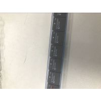
| 类型:通信IC | 电源电压:-55 至 125 | 频率:10HZ |
| 用途:*** | 品牌:AD/亚德诺 | 型号:AD9162BBCZ |
| 封装:法兰封装 | 功率:16W | 特色服务:通信 |
| 批号:16+ |
AD9162BBCZ
16-Bit, 12 GSPS, RF Digital-to-Analog Converters
产品详情
AD9162是一款高性能16位数模转换器(DAC),支持达6 GSPS的数据速率。DAC内核基于一个四通道开关结构配合2倍插值滤波器,使DAC的有效更新速率在某些模式下高达12 GSPS。高动态范围和带宽使这些DAC非常适合最苛刻的高速射频(RF)DAC应用。
在基带模式下,元件的宽带宽能力和高动态范围相结合,在最小两个载波至1.794 GHz的满量程频谱范围内可支持DOCSIS 3.1电缆基础设施兼容性。2倍插值滤波器(FIR85)使AD9161/AD9162针对较低数据速率和转换器时钟进行配置,可降低系统总体功耗和滤波要求。在Mix-Mode? 操作模式中,AD9161/ AD9162可在高达7.5 GHz的二阶和三阶奈奎斯特区内重构RF载波,同时仍保持***动态范围。输出电流可以在8 mA至38.76 mA范围内进行编程。AD9161/AD9162数据接口由最多八个JESD204B串行器/解串器(SERDES)通道组成,可对其通道速度和通道数进行编程,从而实现应用灵活性。
串行外设接口(SPI)可配置AD9162并监控所有寄存器的状态。AD9162提供165引脚、8.0 mm × 8.0 mm、0.5 mm间距、CSP_BGA和169引脚、11 mm × 11 mm、0.8 mm间距、CSP_BGA两种封装,包括引脚选项。
产品特色
高动态范围和信号重建带宽支持高达7.5 GHz的RF信号频率合成。
高达八个通道JESD204B SERDES接口,支持灵活的通道数和通道速度。
带宽和动态范围可满足DOCSIS 3.1余量兼容性要求。
SMJ320C25FDM
This data sheet provides design documentation for the SMJ320C25 and the SMJ320C25-50 digital signal processor (DSP) devices in the SMJ320 family of VLSI digital signal processors and peripherals. The SMJ320 family supports a wide range of digital signal processing applications such as tactical communications, guidance, military modems, speech processing, spectrum analysis, audio processing, digital filtering, high-speed control, graphics, and other computation-intensive applications.
Differences between the SMJ320C25 and the SMJ320C25-50 are specifically identified, as in the following paragraph and in the parameter tables on pages 18 through 24 of this data sheet. When not specifically differentiated, the term SMJ320C25 is used to describe both devices.
The SMJ320C25 has a 100-ns instruction cycle time. The SMJ320C25-50 has an 80-ns instruction cycle time. With these fast instruction cycle times and their innovative memory configurations, these devices perform operations necessary for many real-time digital signal processing algorithms. Since most instructions require only one cycle, the SMJ320C25 is capable of executing 12.5 million instructions per second. On-chip data RAM of 544 16-bit words, on-chip program ROM of 4K words, direct addressing of up to 64K words of external data memory space and 64K words of external program memory space, and multiprocessor interface features for sharing global memory minimize unnecessary data transfers to take full advantage of the capabilities of the instruction set.
Key Features
Military Temperature Range
-55°C to 125°C
100-ns or 80-ns Instruction Cycle Times
544 Words of Programmable On-Chip Data RAM
4K Words of On-Chip Program ROM
128K Words of Data/Program Space
16 Input and 16 Output Channels
16-Bit Parallel Interface
Directly Accessible External Data Memory Space
Global Data Memory Interface
16-Bit Instruction and Data Words
16 × 16-Bit Multiplier With a 32-Bit Product
32-Bit ALU and Accumulator
Single-Cycle Multiply/Accumulate Instructions
0 to 16-Bit Scaling Shifter
Bit Manipulation and Logical Instructions
Instruction Set Support for Floating-Point Operations, Adaptive Filtering, and Extended-Precision Arithmetic
Block Moves for Data/Program Management
Repeat Instructions for Efficient Use of Program Space
Eight Auxiliary Registers and Dedicated Arithmetic Unit for Indirect Addressing
Serial Port for Direct Code Interface
Synchronization Input for Synchronous Multiprocessor Configurations
Wait States for Communication to Slow-Off-Chip Memories/Peripherals
On-Chip Timer for Control Operations
Three External Maskable User Interrupts
Input Pin Polled by Software Branch Instruction
1.6-um CMOS Technology
Programmable Output Pin for Signaling External Devices
Single 5-V Supply
On-Chip Clock Generator
Packaging:
68-Pin Leaded Ceramic Chip Carrier (FJ Suffix)
68-Pin Ceramic Grid Array (GB Suffix)
68-Pin Leadless Ceramic Chip Carrier (FD Suffix)


